Defects in multi-layer 2D materials published in Phys. Rev. B

D. Wang and R. Sundararaman, “Layer dependence of defect charge transition levels in two-dimensional materials”, Phys. Rev. B 101, 054103 (2020)
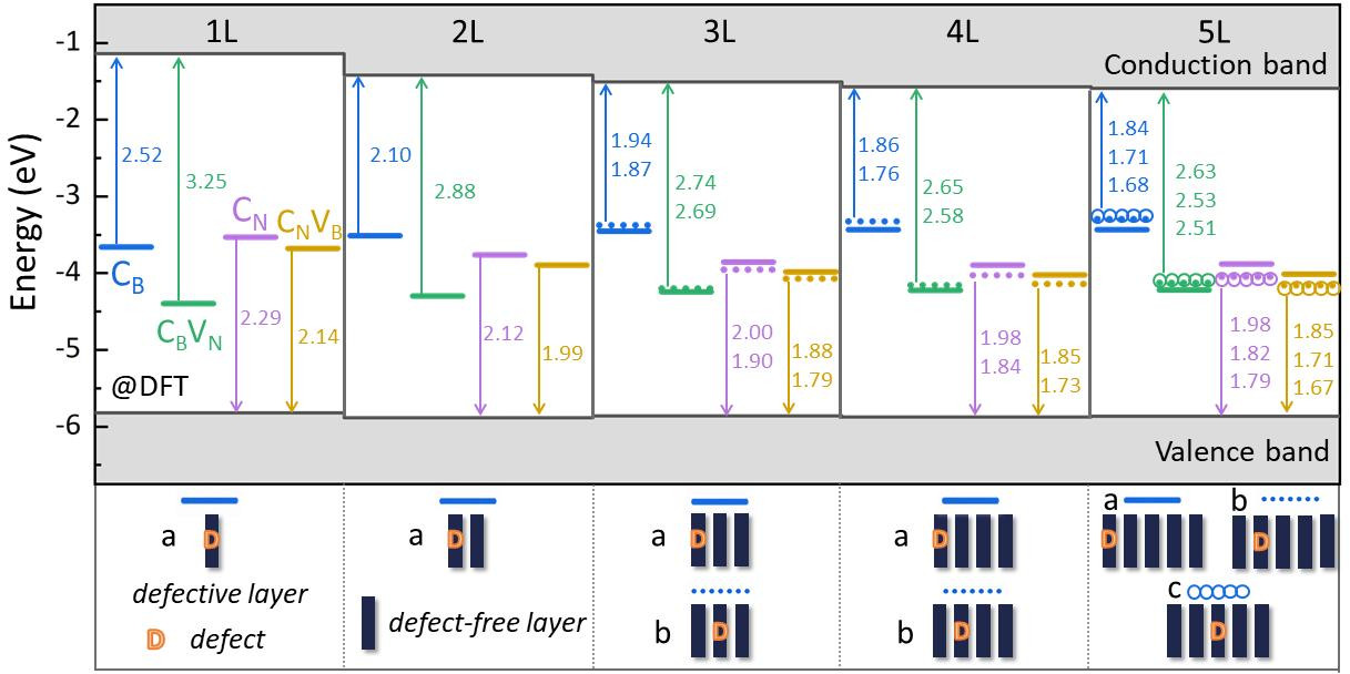
The high sensitivity of two-dimensional (2D) materials to surroundings makes layer number an important consideration in designing devices for opto-electronic and quantum applications. However, the theoretical prediction of how the defect level varies with number of layers and with position within the stack of layers is extremely challenging due to the high computational cost.
In this paper, we demonstrate that defect energies can be accurately and efficiently predicted with a continuum model where only one explicit atomic layer containing the defect is included in the quantum-mechanical calculations, with all remaining defect-free layers replaced by their dielectric response alone. Application of the model to defects in multilayer hBN (from monolayer to five-layer and bulk) systematically reveals the defect transition level dependence on layer number and defect location. This provides a clear quantitative understanding of dielectric effects on defect properties and theoretical guidance on how to tune defect levels in 2D materials using material thickness and defect location within the material.
