Defect engineering in 2D hBN published in Phys. Rev. Mater.
F. Wu, A. Galatas, R. Sundararaman, D. Rocca and Y. Ping, “First-principles engineering of charged defects for two-dimensional quantum technologies”, Phys. Rev. Mater. 1, 071001(R) (2017)
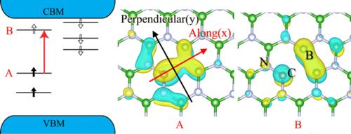
Quantum computers could dramatically change the limits of what we can calculate in the next decade, and the quest for quantum supremacy has already begun! A key step towards ubiquitous quantum computing will be compact solid-state technologies, such as those using nitrogen-vacancy (NV) centers in diamond, compared to the much larger superconducting circuits in use today. In collaboration with Yuan Ping’s group at UC Santa Cruz and Dario Rocca at Université de Lorraine, we predict computationally that similar defect states suitable for quantum computing could exist in two-dimensional boron nitride (2D hBN). In particular, we develop computational techniques to accurately evaluate the stability of such defects and energy levels of various charge states, and use it to identify suitable defect states that can be controlled with light. The prospect of quantum technology in a single-atom-thick material is extremely exciting on account of the potential scale that such a technology could achieve!